As the global demand for renewable energy continues to grow, the photovoltaic (PV) industry is constantly developing technologies that improve solar panel efficiency and long-term performance. Among the most significant innovations is the adoption of N-type monocrystalline silicon wafers, which have become the preferred foundation for next-generation high-efficiency solar cells.
Compared with conventional wafer technologies, N-type monocrystalline silicon wafers deliver higher conversion efficiency, lower degradation, and better long-term power generation. These advantages make them an ideal choice for advanced solar cell technologies such as TOPCon, Back Contact (BC), and other high-performance photovoltaic solutions. Gokin Solar manufactures large-size N-type monocrystalline silicon wafers using advanced Czochralski crystal growth technology and supports multiple wafer formats, including M10, G12, and G12-R.
What Are N-Type Monocrystalline Silicon Wafers?
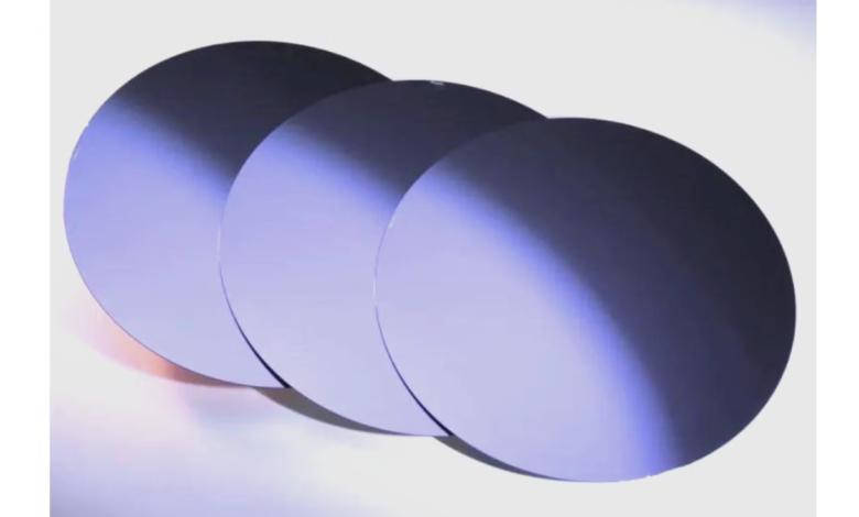
N-type monocrystalline silicon wafers are high-purity silicon substrates produced from single-crystal silicon ingots. Unlike traditional P-type wafers, N-type wafers use phosphorus as the primary dopant, resulting in improved electrical performance and reduced degradation over time.
These wafers serve as the foundation for manufacturing high-efficiency photovoltaic cells and are widely used in utility-scale solar farms, commercial installations, and residential solar systems.

Common characteristics include:
- High-purity monocrystalline silicon
- N-type conductivity
- Large wafer formats
- Thin wafer technology
- Low oxygen and carbon content
- Long carrier lifetime
- High mechanical stability
These features contribute to better overall solar module performance and energy output. Gokin Solar’s N-type wafers feature resistivity of 0.6–1.6 Ω·cm, oxygen content of ≤12 ppma, carbon content of ≤1 ppma, and carrier lifetime of at least 800 μs.
Why N-Type Wafers Are Becoming the Industry Standard
Solar manufacturers are increasingly adopting N-type technology because it offers significant performance advantages over earlier wafer generations.
Key benefits include:
- Higher cell conversion efficiency
- Lower light-induced degradation (LID)
- Improved long-term reliability
- Better temperature performance
- Higher power generation
- Greater compatibility with advanced solar cell technologies
These advantages help reduce the overall cost of electricity while increasing system performance throughout the module’s operating life.
Benefits of N-Type Monocrystalline Silicon Wafers
Higher Energy Conversion Efficiency
N-type wafers support advanced cell structures that convert more sunlight into electricity, enabling higher power output from each solar module.
Lower Performance Degradation
Compared with conventional technologies, N-type wafers experience lower degradation, helping solar panels maintain stable performance for many years.
Excellent Electrical Performance
High carrier lifetime and carefully controlled material quality contribute to improved electrical characteristics and greater energy production.
Large-Format Compatibility
Modern N-type wafers are available in multiple dimensions, allowing manufacturers to optimize module design for residential, commercial, and utility-scale applications.
Reliable Long-Term Performance
Premium manufacturing processes ensure excellent crystal quality, helping improve module durability under various environmental conditions.
Essential Features to Look For
High-Purity Silicon Material
Premium raw materials reduce impurities and improve overall photovoltaic performance.
Advanced Crystal Growth Technology
Manufacturers using the Czochralski crystal growth process can produce highly uniform monocrystalline wafers with excellent electrical properties.
Thin Wafer Manufacturing
Modern thin-wafer technology helps reduce silicon consumption while maintaining mechanical strength and high efficiency.
Strict Quality Control
Reliable manufacturers perform comprehensive inspections to verify wafer dimensions, resistivity, lifetime, and material consistency before shipment.
Multiple Size Options
Large-format wafers such as M10, G12, and G12-R provide flexibility for different module designs and manufacturing requirements.
How to Choose the Right N-Type Monocrystalline Silicon Wafers
Selecting the appropriate wafer supplier is critical for achieving consistent module quality and production efficiency.
Evaluate Manufacturing Experience
Choose manufacturers with proven expertise in monocrystalline wafer production and advanced photovoltaic technologies.
Review Product Specifications
Compare wafer dimensions, resistivity, carrier lifetime, thickness, and impurity levels to ensure they meet your manufacturing requirements.
Consider Production Capacity
Large-scale production capability helps ensure stable supply for long-term manufacturing projects.
Verify Quality Standards
Look for manufacturers that maintain internationally recognized quality management systems and rigorous inspection procedures.
Assess Technical Support
Reliable engineering support and customized solutions can simplify product integration and improve manufacturing efficiency.
Applications of N-Type Monocrystalline Silicon Wafers
N-type wafers are widely used across the photovoltaic industry, including:
- TOPCon solar cells
- Back Contact (BC) solar cells
- High-efficiency photovoltaic modules
- Utility-scale solar power plants
- Commercial rooftop solar systems
- Residential solar installations
- Distributed energy projects
- Renewable energy infrastructure
Their high efficiency and reliability make them a preferred choice for next-generation solar technologies.
Why Choose Gokin Solar?
Gokin Solar is a leading manufacturer specializing in monocrystalline silicon wafers, photovoltaic modules, and integrated solar solutions. Founded in 2019, the company has developed large-scale production capabilities with annual capacities of 100 GW for monocrystalline silicon ingots and wafers and serves customers in more than 30 countries.
Key advantages include:
- Advanced N-type wafer manufacturing
- Large-size wafer technologies
- Czochralski crystal growth process
- M10, G12, and G12-R wafer options
- High carrier lifetime and low impurity levels
- Strict quality management
- Large-scale production capacity
- Continuous research and development
- Global supply network
- Comprehensive photovoltaic solutions
Conclusion
N-type monocrystalline silicon wafers are driving the next generation of photovoltaic innovation by delivering higher efficiency, improved reliability, and superior long-term performance. As the solar industry continues to adopt advanced cell technologies, these wafers provide the foundation for more powerful and cost-effective solar modules.
By partnering with an experienced manufacturer like Gokin Solar, businesses gain access to high-quality N-type wafer solutions backed by advanced manufacturing technology, large-scale production capacity, and comprehensive technical expertise. These advantages help manufacturers build more efficient solar products while supporting the global transition toward clean and sustainable energy.